Coding the approach to next-gen transistors
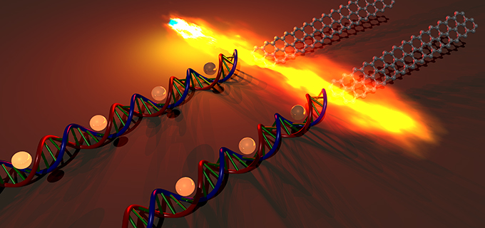
Research published in the new Nature Communications journal proposes building the next generation of transistors and computer chips out of graphene assembled by strands of DNA.
The futuristic concept has been discussed by Stanford chemical engineering professor Zhenan Bao and co-authors, former post-doctoral fellows Anatoliy Sokolov and Fung Ling Yap.
The scientists are taking the first step in tackling a big issue on the horizon for engineers – what to do now that traditional silicon chips have been pushed to the very threshold of their physical capability for switch-making.
Currently in transistors and computer chip design; manufacturers have concentrated much electricity in an ever-diminishing space, producing small, faster, cheaper chips. However, these gates and switches are so tiny that heat and other forms of interference can disrupt the inner workings.
“We need a material that will let us build smaller transistors that operate faster using less power,” Bao said.
The team believes that ribbons of graphene, laid side-by-side, could create semiconductor circuits. Given the material's tiny dimensions and favourable electrical properties, graphene nano-ribbons could create ultra-fast chips that run on minimal power.
“However, as one might imagine, making something that is only one atom thick and 20 to 50 atoms wide is a significant challenge,” said co-author Sokolov.
Tackling the issue of thickness is where the team brought in another cutting-edge field of science; custom DNA sequencing and cellular design.
DNA strands were employed for the task due to a number of advantages; they are long and thin, exist in roughly the same dimensions as the graphene ribbons and contain carbon atoms - the material that forms graphene.
The team managed to create a transistor through a complicated process of embedding bacteria in a platter, exposing it to a copper salt solution (which absorbed copper ions into the DNA), and bathing it in methane gas to add carbon atoms.
“The loose carbon atoms stayed close to where they broke free from the DNA strands, and so they formed ribbons that followed the structure of the DNA,” Yap said.
“We demonstrated for the first time that you can use DNA to grow narrow ribbons and then make working transistors,” Sokolov said.
UC Berkeley associate professor Ali Javey, an expert in the use of advanced materials and next-generation electronic devises said: “This technique is very unique and takes advantage of the use of DNA as an effective template for controlled growth of electronic materials... the project addresses an important research need for the field.”
All reports from the latest edition of Nature Communications are available here.


 Print
Print